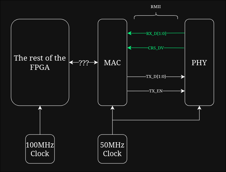
In digital design, designers prefer to design digitally. The physical layer transceiver (PHY) handles the non-digital parts of Ethernet communication, and exposes a digital interface to the rest of the system.
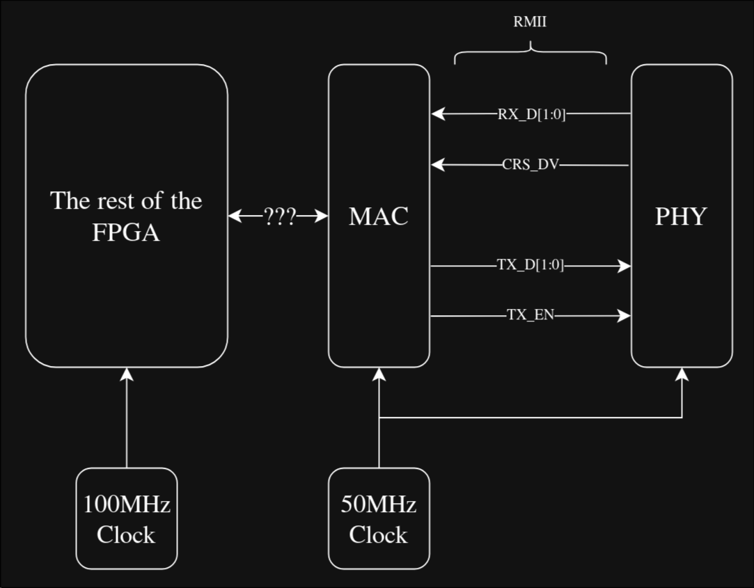
The component that bridges the gap between the PHY and everything else is the Ethernet MAC (Media Access Controller). The digital interface between the MAC and the PHY used by the Nexys A7 is the Reduced Media Independent Interface (RMII). The datasheet section of my local public library had a document for it: RMII Specification.
On the other side of the elf-provided diagram, there was another diagram:
RMII operates with a 50MHz reference clock. The FPGA board uses a 100MHz clock. 50 is not 100, nor vice versa. So it's up to me to find a way to generate a 50MHz clock and share it with the PHY.
A simple solution would be to maintain a 1-bit counter that increments on every 100MHz clock cycle, which would then effectively output half the frequency of the input clock. That could work, and for many designs doing that sort of thing is fine. But for clock signals, details like routing, startup behavior, and how vendor tools treat the signal start to matter more. Vivado provides a dedicated Clocking Wizard IP that handles these details explicitly, so I'll be using that here.
             ^
         o  {0}
        / \  V
       (*_*) |  I can generate many clocks,
         |   |  for the price of a clock.
       \-----|
         |   |
        / \  ^
Given an input clock of 100MHz and a reset signal, the Clocking Wizard will output a 50MHz clock. The Wizard is also capable of generating multiple clocks of differing frequencies at differing phases. It can even generate a clock with a higher frequency than the input clock. But I don't need those capabilities right now.
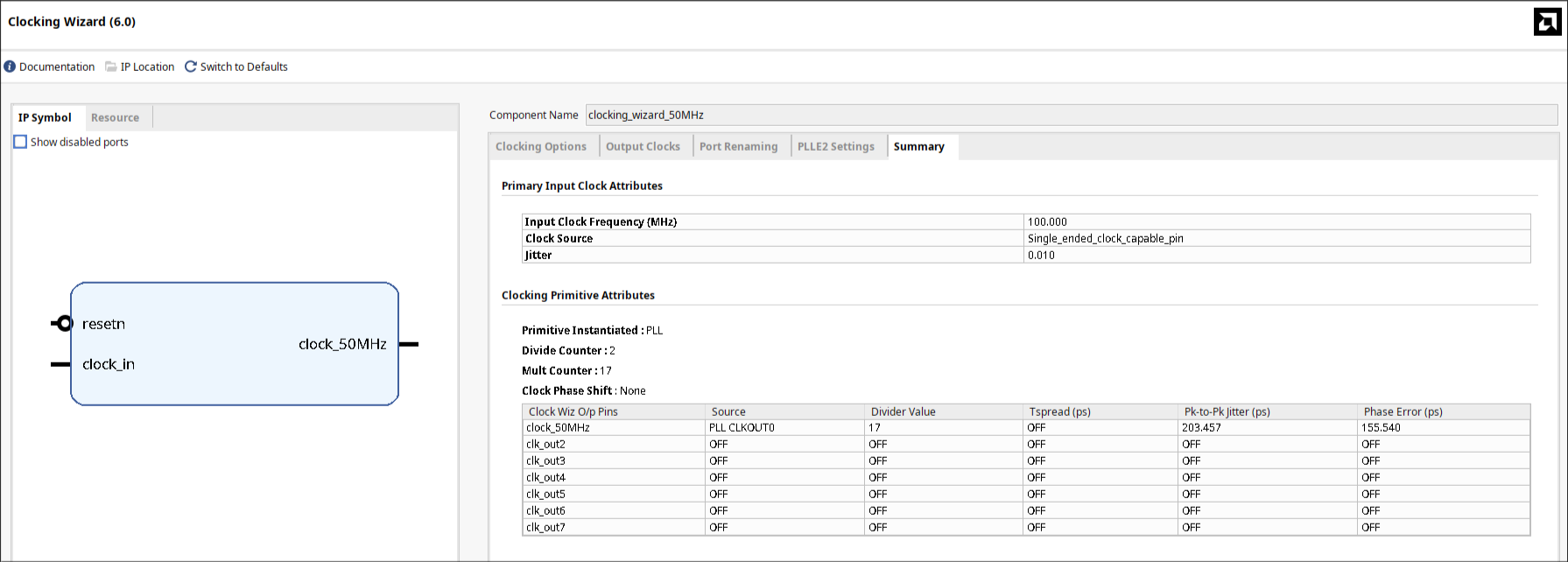
After adding an IP Core to your design, Vivado provides a template to instantiate that design into your RTL. However, the templates provided are in Verilog and VHDL. Hardcaml is neither of those, so some adjustments were necessary. Here is the template provided by Vivado:
        //----------- Begin Cut here for INSTANTIATION Template ---// INST_TAG

        clocking_wizard_50MHz instance_name
        (
          // Clock out ports
          .clock_50MHz(clock_50MHz),     // output clock_50MHz
          // Status and control signals
          .resetn(resetn),               // input resetn
          // Clock in ports
          .clock_in(clock_in)            // input clock_in
        );

        // INST_TAG_END ------ End INSTANTIATION Template ---------
And here is the corresponding Hardcaml:
        let clocking_wizard_50MHz =
          Instantiation.create
            ~name:"clocking_wizard_50MHz"
            ~inputs:[ "clock_in", clock; "resetn", reset_n ]
            ~outputs:[ "clock_50MHz", 1 ]
            ()
        in
        let clock_50MHz = Instantiation.output clocking_wizard_50MHz "clock_50MHz" in
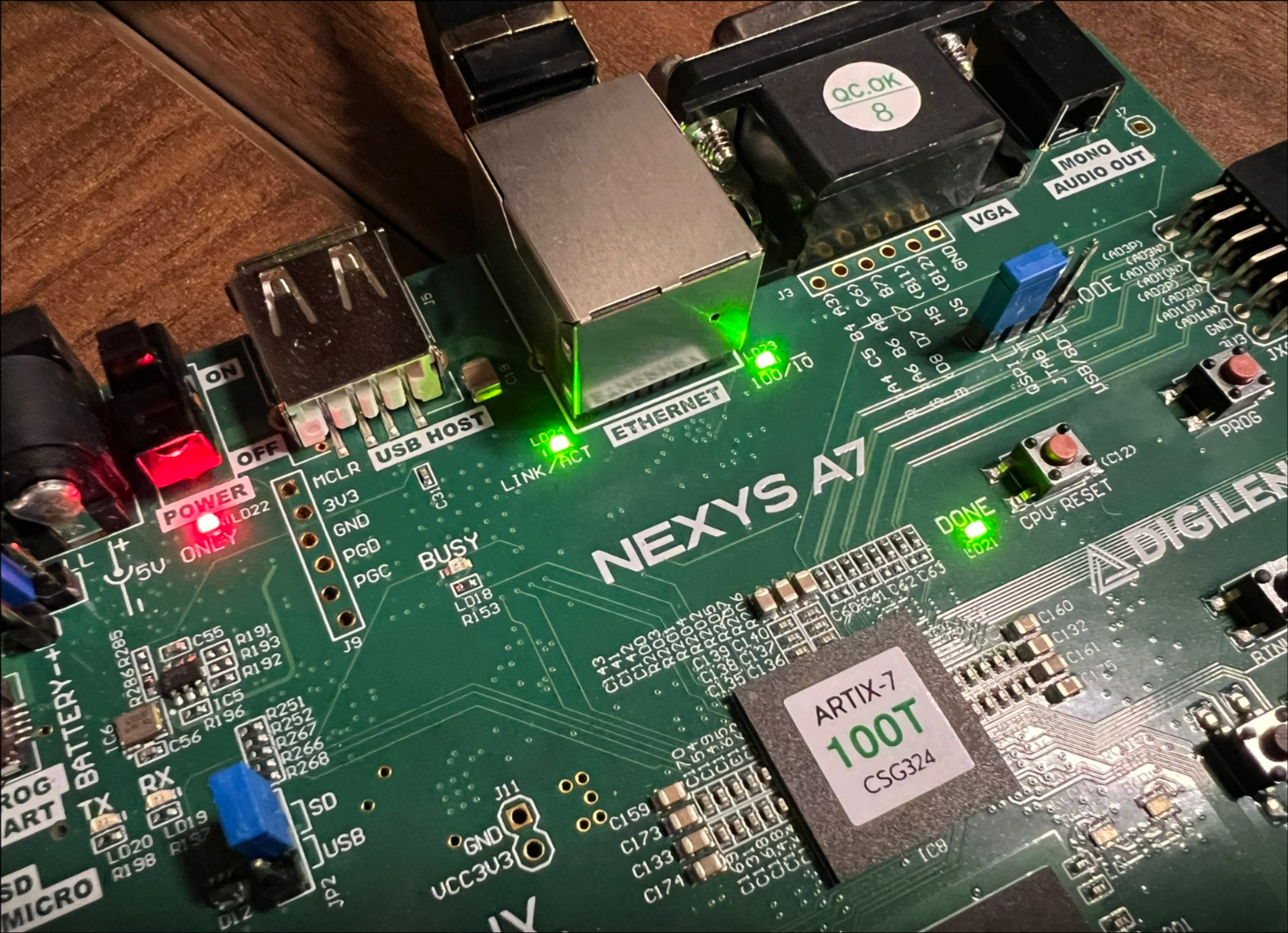
Once the 50MHz clock is provided to the PHY, it will automatically manage link/activity status and speed negotiation. After programming the FPGA with a very simple design that just routes the 50MHz output from the Clocking Wizard IP Core to the PHY, the status lights (which are controlled by the PHY) have lit up. Great success.
Communication from the PHY to the MAC happens with two main signals: RX_D and CRS_DV. RX_D is the data signal and is 2 bits wide, which I will refer to as a dibit (also known as a crumb (a crumb is half of a nibble (a nibble is half of a byte))). Without getting into the details, CRS_DV can be considered a "valid" signal, indicating that RX_D is non-idle and contains valid bits.
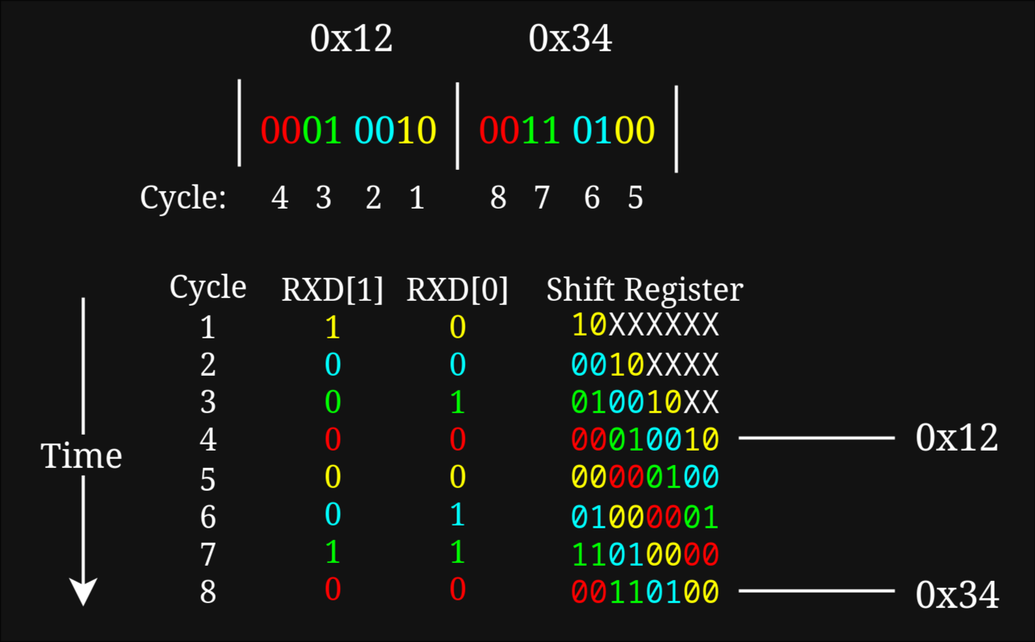
Since RX_D is only 2 bits wide, I want to pack it into wider values before further processing. But this raises the question: How are the byte boundaries defined? Maybe the byte boundaries begin as soon as CRS_DV is asserted. Maybe not. But there's a way to know for sure, and this requires knowing a bit about how ethernet frames are constructed.
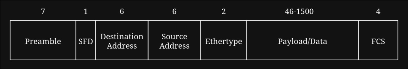
The start of an Ethernet frame is marked by a Preamble followed by a Start Frame Delimiter (SFD). The Preamble is a 7-byte sequence of alternating 0s and 1s. The Start Frame Delimiter is 1 byte and continues the pattern of the Preamble but concludes with two adjacent 1s. Grouped by dibits, it looks like this:
01 01 01 01 01 01 01 01 ... 01 01 01 11
We can check for this pattern by reading the input into a 64-bit shift register and checking on every cycle. Once the start of frame is detected, the MAC knows it's on a byte boundary and can begin processing the rest of the Ethernet frame.
As an example, suppose the value 0x1234 is being transmitted from the
PHY to the MAC. It is split
into octets first. Then each octet is split into 4 dibits and transmitted
least-significant dibit first. So RX_D[1:0] is shifted in from the left
and on every 4th cycle, I assert a "valid" signal to indicate that the
byte has been constructed.
As a first test of Ethernet frame parsing, let's try to determine if my FPGA can see the MAC address of my desktop computer. Both devices are on the same local network.
First, I ran ip addr to list my computer's network interfaces.
Under the enp3s0 Ethernet interface, I see
link/ether 22:44:66:ab:cd:ef, which is the value I spoofed
my computer's MAC address to be.
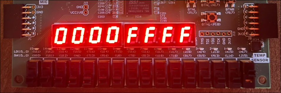
Using the deserialization I described in the previous section, I programmed my FPGA to read every incoming Ethernet frame, load the MAC source address into a register, and display it on the 7-segment display.
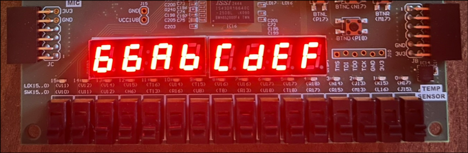
It worked! This confirms that:
Every few seconds, the address displayed here would change to another address
among a small set of addresses. This suggests that each device on my local network is
occasionally sending messages to the FPGA. Or, more precisely, since
these devices aren't aware of my FPGA, these are probably broadcast
messages. I'll test this hypothesis by displaying the MAC Destination address instead
of the Source address. A special MAC address is reserved for broadcast signals:
FF:FF:FF:FF:FF:FF.
Let's see...
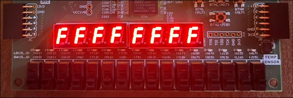
Yup.
But what are these occasional messages for? The answer lies in the remaining fields of the Ethernet frame. I'll do that later.
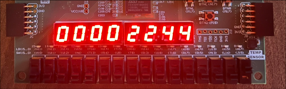
Okay it's later. I programmed the FPGA to display the 2-byte Ethertype field and every few seconds it switches between a set of 3 values, which correspond to the following types of frames: